Inquiry
Form loading...

10 Essential Tips for Understanding Ito Thin Film Technology?

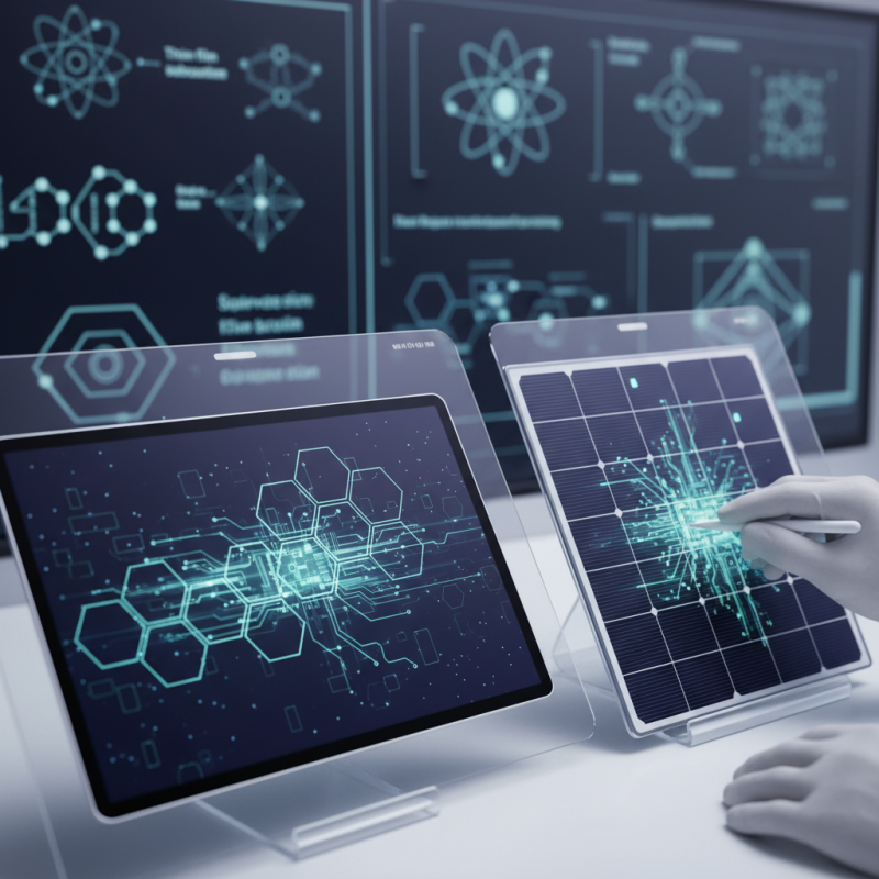
Understanding Ito Thin Film technology is crucial in today’s fast-paced electronics market. This technique plays a vital role in applications like touch screens and solar cells. Recent industry reports indicate a projected growth rate of 9.6% in the thin film sector by 2026. Experts like Dr. Emily Roberts emphasize its importance, stating, “Ito Thin Film is at the core of innovations in display technologies.”

However, grasping the nuances of Ito Thin Film can be challenging. Many professionals overlook critical aspects, leading to inefficiencies. The specifications of thin film coatings, for example, require precise calibration to ensure optimal performance. Additionally, the material's properties can differ based on deposition techniques, which complicates the understanding even further.

Staying updated on trends and technologies in Ito Thin Film is essential. Yet, many in the field struggle to keep up with rapid advancements. Continuous learning and collaboration with peers can foster a deeper understanding. Addressing knowledge gaps is crucial for leveraging the full potential of this innovative technology.

10 Essential Tips for Understanding Ito Thin Film Technology?

Introduction to Ito Thin Film Technology

10 Essential Tips for Understanding Ito Thin Film Technology?

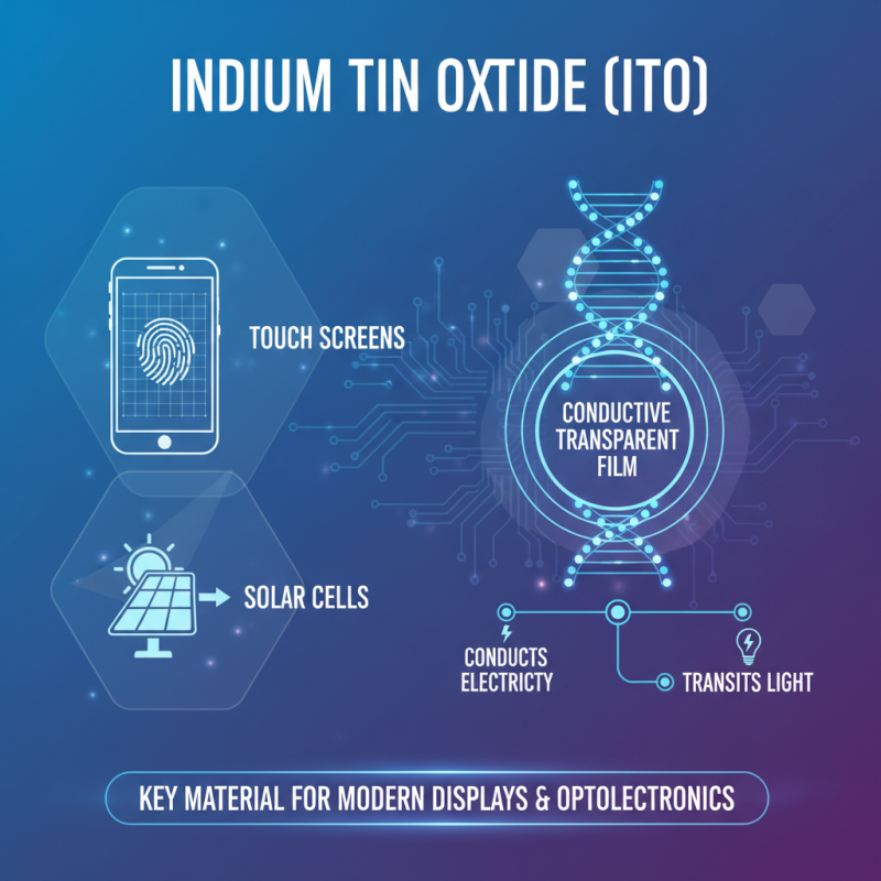
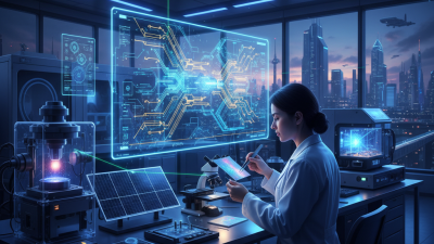
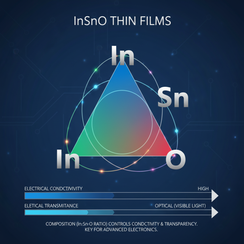
ITO, or Indium Tin Oxide, is a conductive transparent film. This technology is widely used in electronics and optoelectronics. It is a key material for touch screens and solar cells. The unique properties of ITO allow it to conduct electricity while still letting light pass through. This makes it indispensable for modern displays.

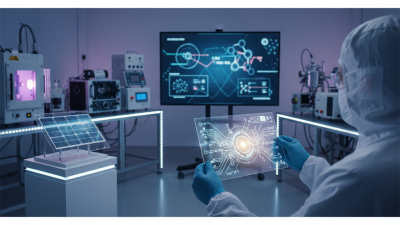
Understanding ITO thin film technology requires a closer look at its production. The process involves sputtering or thermal evaporation techniques. These methods create thin layers with specific thicknesses. However, achieving uniformity can be challenging. Uneven layers can lead to inconsistent performance in devices.

Moreover, the environmental impact of ITO production should not be overlooked. Sourcing indium involves mining, which has ecological consequences. The industry is also exploring alternatives, but solutions are limited. As technology advances, the balance between performance and sustainability remains a crucial concern in ITO thin film technology.

Key Applications of Ito Thin Films in Modern Electronics

Indium tin oxide (ITO) (ITO) thin films play a critical role in modern electronics. They are widely used as transparent conductive materials in a variety of devices. This includes touchscreens, flat-panel displays, and solar cells. Their unique combination of electrical conductivity and optical transparency makes them invaluable.

When considering ITO thin films, it’s essential to understand their applications. In touchscreens, they enable clear visuals while allowing for user interaction. In solar cells, they improve energy conversion efficiency. This technology is crucial for renewable energy advancements.

Tip: Recognize the importance of film thickness. The thickness affects conductivity and transparency. Typically, thinner films enhance light transmission but may reduce conductivity.

Another tip involves examining the deposition techniques used. Techniques like sputtering and chemical vapor deposition can influence film quality. Understanding these nuances is key to harnessing ITO effectively. Embracing these complexities requires a mindset of continuous exploration.

Understanding the Composition and Structure of Ito Films

10 Essential Tips for Understanding Ito Thin Film Technology?

Ito thin films consist mainly of indium, tin, and oxygen. Their unique composition gives them excellent conductive properties. The ratio of these elements is crucial. Different compositions lead to variations in conductivity and optical transmittance. This can impact the performance of devices where Iso films are utilized.

The structure of Ito films plays a significant role as well. Typically, they are deposited in thin layers. These layers can vary in thickness, often ranging from a few nanometers to several micrometers. The deposition technique also matters; it affects grain size and film uniformity. Not all methods produce high-quality films. Some trials may lead to inconsistencies.

Creating high-performance Ito films involves balancing these factors. Researchers must navigate trade-offs between conductivity, flexibility, and thickness. Sometimes, the optimal solution isn't clear. Therefore, iterative testing becomes essential for improvement. Repeated evaluations can unveil hidden issues that need addressing. Emphasizing these nuances can lead to better understanding and advancements in Ito technology.

Advantages of Using Ito Thin Films in Display Technology

Indium Tin Oxide (ITO) thin films are pivotal in display technology. They offer transparency and electrical conductivity, making them ideal for touch screens and flat panel displays. According to industry reports, ITO films can achieve up to 90% optical transparency while maintaining a low resistivity of about 10^-4 ohm-cm. This balance is crucial for modern electronic devices.

The advantages of using ITO thin films extend beyond just visual clarity. Enhanced flexibility in manufacturing processes allows for various applications. Recent studies indicate that ITO coatings enhance the durability of touch interfaces, leading to longer device lifespans. However, there are challenges, such as susceptibility to damage and the potential for limited supply of indium.

Certain alternatives are being researched, but none have matched ITO's performance in key areas. Costs can be an issue as well. It is essential to find ways to recycle and reuse ITO to reduce environmental impact. In exploring ITO technology, careful consideration of its pros and cons helps drive innovation.

10 Essential Tips for Understanding ITO Thin Film Technology

This chart illustrates the advantages of using ITO thin films in display technology across various parameters such as conductivity, transparency, and cost-effectiveness.

Challenges and Future Directions in Ito Thin Film Research

The realm of ITO thin film technology is evolving, yet it faces distinct challenges. Recent reports highlight that the global ITO market is projected to reach $4.5 billion by 2027, driven by advancements in display technologies and photovoltaics. However, researchers still grapple with durability and cost issues. Achieving stable conductivity while minimizing material use remains a hurdle.

Understanding the thin film deposition process is vital. Tip: Maintain optimal deposition parameters to enhance performance. This includes temperature, pressure, and deposition rate. Minor adjustments can lead to substantial differences in film quality. Exploring alternative materials is also promising. Graphene and carbon nanotubes are gaining attention as potential substitutes, but extensive studies are needed to ensure viability.

Additionally, researchers must address recycling ITO materials post-use. Currently, the recycling processes are inefficient. Tip: Prioritize sustainability in research to minimize waste. The cycle of production and disposal is crucial for environmental impact. Future innovations should integrate green technology to forge a path forward. Striving for these improvements will be key in determining the future of ITO thin films.

10 Essential Tips for Understanding Ito Thin Film Technology - Challenges and Future Directions in Ito Thin Film Research

Tip Description Challenges Future Directions
1. Understanding Film Deposition Methods Explore techniques like sputtering and thermal evaporation for ITO films. Uniform thickness and composition control can be challenging. Advancements in real-time monitoring technologies.
2. Characterizing Electrical Properties Learn about resistivity and charge carrier concentration measurement methods. Variability in measurements due to environmental factors. Utilization of standardized testing protocols.
3. Enhancing Optical Properties Study transmission and reflection characteristics of ITO films. Trade-offs between transparency and conductivity. Development of novel dopants to improve both properties.
4. Investigating Thermal Stability Evaluate performance under high-temperature conditions. Degradation of properties over prolonged exposure to heat. Research on more thermally resistant materials.
5. Addressing the Environmental Impact Consider the sustainability of ITO production and recycling. Environmental regulations and supply chain issues. Pursuit of alternative materials to replace ITO.
6. Tailoring Film Morphology Control grain size and surface roughness for better performance. Achieving a consistently desired morphology is complex. Emerging methods in nanostructure engineering.
7. Exploring Applications Beyond Displays Investigate uses in solar cells, sensors, and smart windows. Market acceptance and integration into existing technologies. Innovations in hybrid technologies incorporating ITO.
8. Optimizing Thickness for Functionality Find the optimal thickness for conductivity and transparency. Thickness variations affecting performance in applications. Utilization of computational modeling for optimization.
9. Understanding Aging Effects Assess long-term stability and performance changes. Environmental exposure can drastically impact properties. Development of more durable formulations.
10. Networking with Research Community Engage with peers to share findings and ongoing research. Limited interdisciplinary collaboration in research. Encouragement of collaborative interdisciplinary projects.